05/2025 Spectacular success at the E-MRS Spring Meeting 2025 in Strasbourg: Lukas Gehrig won the "Best Poster" award, Jonas Erhardt the "Best Oral Contribution" award of the Symposium on "Topological Materials". Congratulations!! Atomic monolayers rule!!
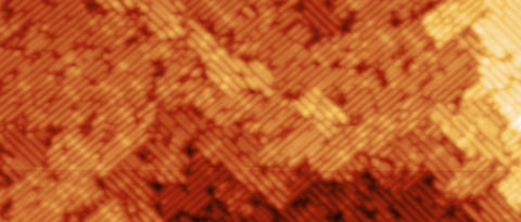
05/2025 New paper on "Bismuthene under cover: graphene intercalation of a large gap quantum spin Hall insulator" in Advanced Materials.
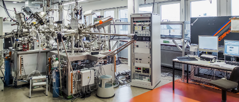
05/2025 Another new paper that just appeared in Ultramicroscopy provides a comprehensive description (including test data) of our novel momentum microscope "SAMMy" at the Diamond Light Source, UK.
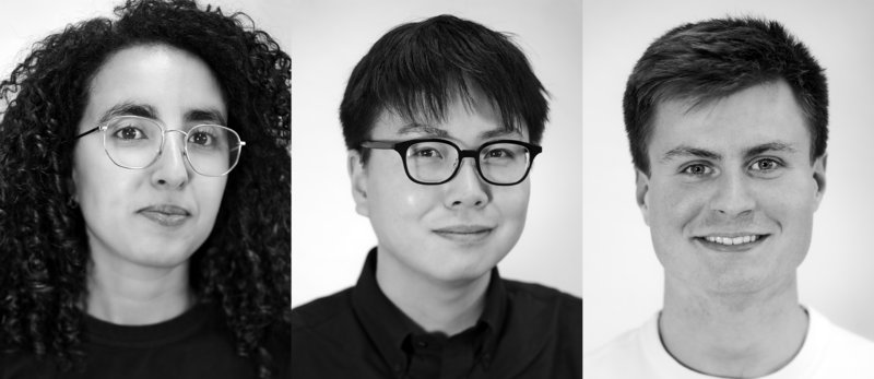
05/2025 We are happy to welcome three new EP4 members to the Claessen group; from left to right: Dr. Houda Koussir--new postdoc in the Nanoteam (from U Lille, France), Dr. Goro Nozue--new postdoc in the Oxide Team (from U Osaka, Japan), and Florian Giletta--summer intern (from U Paris-Saclay, France).